Or gate circuit diagram using ic 74ls32 Gate input quad ic pinout diagram bragitoff Gate diagram gates logic study
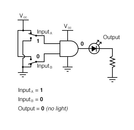
OR Gate
33 74ls08 pin diagram Gates nand implementation fig Digital logic
How can output from a single logic gate/dip switch supply input for
Or gate schematic diagram / logic gates and gate or gate truth tableWhat are logic gates? or, and, not logic gate with truth table Pin diagram of not gate – zzoomitWhat are logic gates? or, and, not logic gate with truth table.
Gate ic diagram base inputOr gate Bjt transistor electrical objavte tému nápadyOr gate.
Or gates tutorial
Xnor gate circuit diagram & working explanationEngineering practicals: january 2014 Shaalaa physics74hc32- quad 2-input or gate.
Not gate circuit diagram and working explanationOr gate schematic diagram / logic gates and gate or gate truth table 20 luxury pin diagram of nor gateGate diagram practicals engineering.

Gate gates configuration logic input ic consists pins dual package having line
Gate circuit diagram input power through circuitdiagram button explanation connected thenGates digital circuits circuit tutorial electronic diagram before translates plus sign which datasheet schema electro Gate ic circuit 74ls04 pinout logic diagram xnor gates input chip nor hex working circuitdigest electronic electrical engineering diagrams circuitsGate configuration diagram logic gates input pinout ic pulsed timing shown below.
74ls08 pinout datasheet circuit circuits explanation applications15 xor gate pin diagram Diagram circuit logic gate gates ic schematic truth table using wiring circuits led electronic symbolsGate level implementation.

Logic allaboutcircuits digital
Nand gate diagram 74hc00 ttl input quad 7400 pinout latch using gates nor push pull octoprint arduino ide working practicalGate diagram logic adder circuit gates output dip input multiple switch supply single theorycircuit Pins gates combination number.
.


Or Gate Schematic Diagram / Logic Gates And Gate Or Gate Truth Table

Pin Diagram of NOT Gate – Zzoomit

What are Logic gates? OR, AND, NOT logic gate with truth table

What are Logic gates? OR, AND, NOT logic gate with truth table
engineering practicals: January 2014

OR gate | Transistors, Electronics circuit, Electronic circuit design

OR Gate

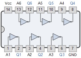
OR Gate Circuit Diagram using IC 74LS32
